

Photomask Inspection Market Demand Accelerates Due to Precision Lithography and Semiconductor Complexity Growth
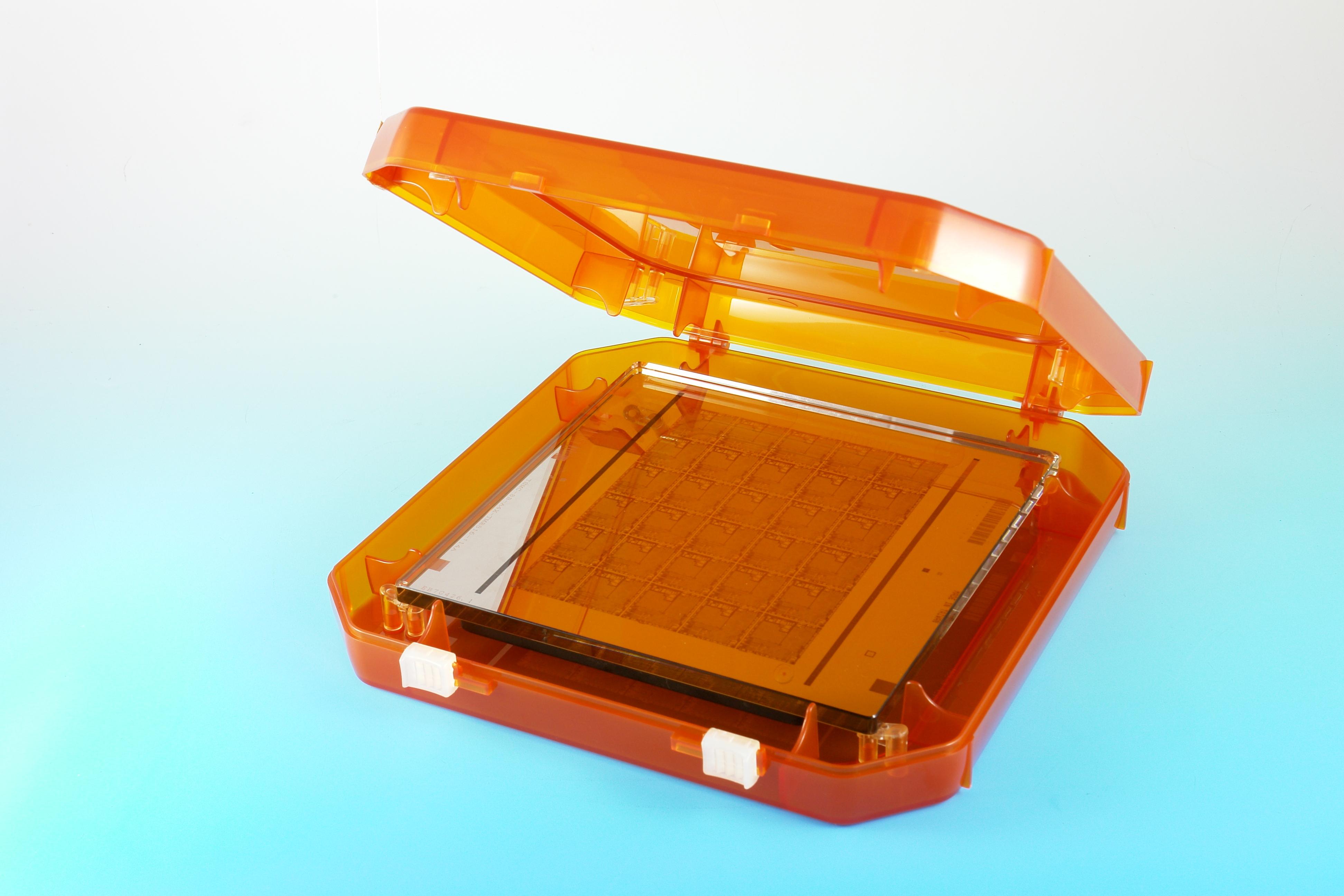
The photomask inspection market is witnessing a significant surge in demand, propelled by the rapid evolution of semiconductor manufacturing and the need for heightened accuracy in microchip production. Photomasks are foundational to the lithography process, where intricate patterns are transferred onto silicon wafers to build integrated circuits. As consumer electronics, automotive systems, and industrial applications demand ever-smaller and more powerful chips, the photomask inspection process becomes increasingly vital for ensuring defect-free pattern replication.
The growing demand for high-performance computing, smartphones, IoT devices, and 5G technologies has led to shrinking node sizes, with manufacturers now pushing boundaries toward the 2nm process and beyond. At these nanoscale levels, even the tiniest defect on a photomask can result in critical device failure or reduced yield. As a result, the market is experiencing a spike in demand for advanced inspection tools that can detect sub-micron defects with exceptional accuracy.
One of the primary drivers behind the increasing demand is the adoption of extreme ultraviolet (EUV) lithography. EUV has transformed the semiconductor manufacturing landscape by allowing for finer patterning with shorter wavelengths. However, this also introduces new challenges in photomask production and inspection, as EUV masks have different properties compared to traditional ones. The sensitivity of EUV masks to contaminants and distortions has necessitated the use of specialized inspection systems capable of operating at EUV wavelengths. This shift is creating a consistent and growing demand for high-end photomask inspection solutions compatible with EUV processes.
Another factor amplifying demand is the move toward complex chip architectures, such as 3D stacking, heterogeneous integration, and advanced packaging. These techniques, while improving performance and efficiency, require highly precise alignment and pattern fidelity across multiple layers. This complexity increases the burden on photomasks and heightens the need for robust inspection systems to ensure pattern integrity. As a result, chipmakers and foundries are investing heavily in inspection tools to maintain their competitive edge and meet production goals.
In parallel, the industry is witnessing a rising preference for automated and real-time inspection systems. Traditional off-line inspection methods, though reliable, often introduce delays in the production process. Today’s fabs are increasingly integrating in-line inspection tools that allow for real-time defect detection and immediate feedback, minimizing costly downtime and reducing the risk of defective batches. This transition toward automation aligns with broader smart manufacturing trends and has become a key contributor to the growing demand for photomask inspection technologies.
Additionally, increased investment in semiconductor fabrication facilities globally is boosting market demand. Nations such as the U.S., China, South Korea, and members of the European Union are ramping up efforts to establish a resilient and self-sufficient semiconductor ecosystem. This includes funding new fabs and upgrading existing ones with state-of-the-art tools. Photomask inspection is a critical part of this infrastructure, and with the global push toward semiconductor independence, demand for inspection systems is expected to remain robust for the foreseeable future.
The rise in demand is not only restricted to advanced nodes. Even legacy and mid-range nodes are experiencing inspection tool demand due to their continued relevance in automotive electronics, industrial equipment, and consumer devices. While these nodes may not require the same level of inspection resolution as advanced nodes, they still depend on reliable photomask quality to ensure product reliability. Consequently, inspection tool manufacturers are developing versatile solutions that cater to both ends of the spectrum.
Furthermore, increasing emphasis on yield enhancement and cost efficiency is influencing purchasing decisions within semiconductor companies. A single undetected photomask defect can result in wafer yield loss, impacting profitability and delivery timelines. As the cost of semiconductor production continues to climb, especially with cutting-edge nodes, manufacturers are prioritizing investments in inspection equipment that ensures high first-pass yield and defect-free output. This economic imperative is creating a strong business case for deploying advanced photomask inspection systems across all major fabs.
On the competitive front, the photomask inspection market is experiencing intense activity among leading vendors and emerging players. Companies are innovating aggressively, offering solutions with higher resolution, AI-driven analytics, and enhanced throughput. Strategic alliances and acquisitions are also playing a role, as firms seek to expand their technological portfolios and global footprint to meet surging demand from semiconductor customers.
In conclusion, the demand for photomask inspection tools is being driven by a combination of factors including advanced lithography, semiconductor miniaturization, complex chip architectures, and global fabrication expansion. As the semiconductor industry continues to evolve rapidly, the importance of photomask inspection as a quality control pillar is growing stronger. Companies that invest in next-generation inspection technologies will be better positioned to deliver reliable, high-performance chips in an increasingly competitive marketplace.